A field map of the chip industry — 2026
Semiconductors have stopped being just “an IT component.” They are now a national economic-security asset. A single smartphone contains dozens of different chip types, and a modern electric vehicle uses well over a thousand. Yet surprisingly few people have a clear picture of how a chip actually gets made — or how it ends up inside the products we use every day.
This report starts at silicon (literally, sand) and follows the chain all the way to finished products, stopping along the way at the “brain chips” — GPUs, NPUs, and TPUs — and the foundries, like TSMC and Samsung, that physically manufacture them. It closes with a practical look at two questions readers keep asking: what does the rare-earth story actually mean for chips, and how does an ordinary person actually get into this industry.
01 · The Map: Eight Links in One Global Chain
A chip is never made in a single factory. It’s closer to a relay race run by companies scattered across the globe, each handing off to the next.
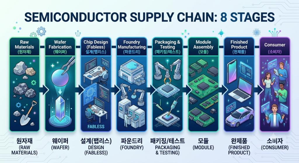
Raw materials → Wafers → Design (fabless) → Foundry (fabrication) → Packaging & testing (OSAT) → Modules/components → Finished products → End users
If any single link in this chain breaks, the whole thing stops. Japan’s 2019 hydrogen fluoride export restrictions, the 2020–22 pandemic-driven automotive chip shortage, and today’s rare-earth and specialty-gas tensions between the US and China all point to the same lesson: the real vulnerability isn’t in the finished product — it’s several steps upstream, in places most people never think about.
02 · Upstream: A Chip Is, in the End, Purified Sand
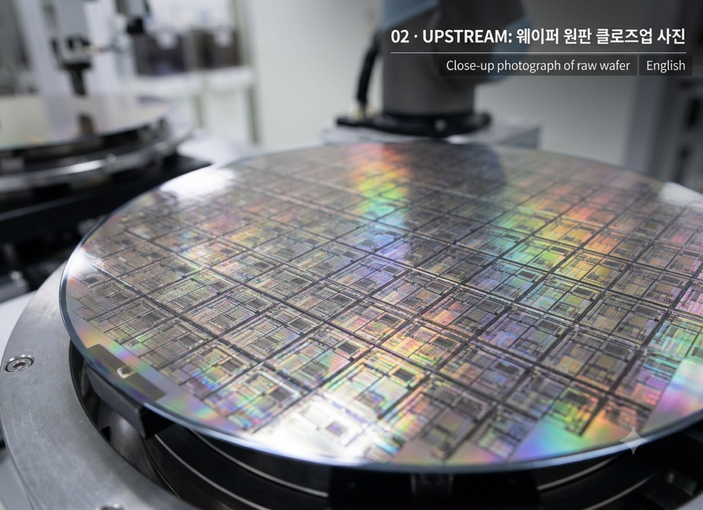
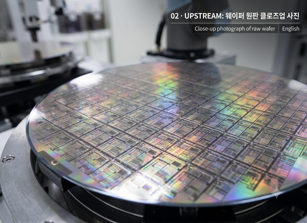
The raw material behind every semiconductor is silicon (Si) — an element that’s actually abundant in ordinary sand and quartz. Silicon is extracted, purified to “nine nines” (99.9999999%) purity, grown into a cylindrical crystal ingot, and sliced paper-thin into wafers. That’s where the story begins.
| Material | Role | Key Players | Notes |
|---|---|---|---|
| Polysilicon / wafers | The base substrate for every chip | Shin-Etsu Chemical, SUMCO, SK Siltron, GlobalWafers | 300mm wafers dominate; AI demand is straining supply |
| Photoresist | Light-sensitive chemical used to etch circuit patterns | JSR, Shin-Etsu, TOK | Central to the 2019 Japan–Korea export dispute |
| Specialty gases (neon, argon, etc.) | Medium for lithography lasers and plasma etching | TEMC, Air Liquide, Linde | Supply-chain risk rose sharply after the war in Ukraine |
| Hydrofluoric acid & ultra-pure chemicals | Wafer cleaning and etching | Stella Chemifa, Morita Chemical, Soulbrain | Purity qualification can take months to years |
| Rare earths & specialty metals | Compound semiconductors, wiring, thermal materials | Dominated by Chinese refiners | China’s leading export-control lever (see Section 09) |
| EUV lithography systems | Ultra-fine-line lithography equipment | ASML (Netherlands) — effectively a monopoly | Roughly €250–300 million per machine |
The materials layer is unglamorous but irreplaceable. If one of these inputs is blocked, the entire fab stops — not just slows down.
03 · Taxonomy: Two Broad Families — Memory and Logic
The simplest way to think about semiconductors is “chips that remember” versus “chips that think.”
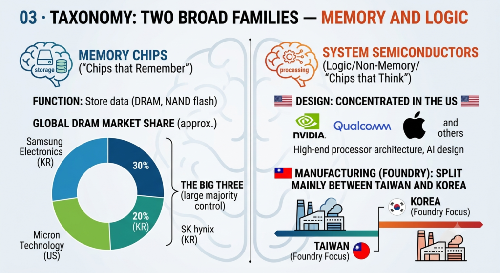
- Memory chips store data (DRAM, NAND flash). This is the arena where Korea’s Samsung Electronics and SK hynix rank first and second globally, with US-based Micron Technology rounding out the “big three” — the three companies together control the large majority of the world’s DRAM output.
- System (logic/non-memory) semiconductors process data. Design is concentrated in the US (Nvidia, Qualcomm, Apple, and others), while manufacturing (foundry) is split mainly between Taiwan and Korea.
04 · Brains: GPU, NPU, and TPU — Three Kinds of AI Chip
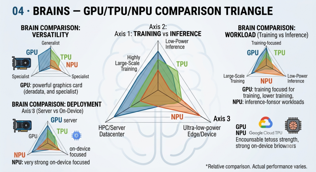
All three chip types accelerate AI computation, but they diverge along three axes: general-purpose vs. specialized, training vs. inference, and data center vs. the device in your hand.
| GPU | TPU | NPU | |
|---|---|---|---|
| Original purpose | Graphics rendering, later extended to AI training | Purpose-built ASIC for Google’s AI workloads | Purpose-built for on-device neural-network inference |
| Strength | Large-scale training, general-purpose parallel compute | Extremely fast inference/training within a specific framework | Low-power, low-latency inference |
| Power profile | High performance, high heat | Server-grade power, optimized for efficiency | Ultra-low power (battery-optimized) |
| Typically found in | Data centers, gaming, supercomputers | Inside Google Cloud | Smartphones, laptops, cars, IoT devices |
| Example | Nvidia H100 / Blackwell | Google TPU v6 (Trillium) | Apple Neural Engine, Qualcomm Hexagon |
05 · Foundry: “Just Bring Us the Design, We’ll Print It”
Companies like Nvidia, Qualcomm, and Apple design chips but don’t build their own factories. These design-only companies are called fabless, and the specialized contract manufacturers that turn their blueprints into physical wafers are called foundries.
| Foundry | 2026 status | Key customers |
|---|---|---|
| TSMC (Taiwan) | Leading with 2nm (N2) yields around 70–80%; production lines already running at capacity | Apple, Nvidia, AMD, and others |
| Samsung Foundry (Korea) | Chasing with 2nm GAA yields around 50–60%; landed a major Tesla AI6 order | Tesla, Qualcomm (in negotiation), IBM, Rebellions |
| Intel Foundry (US) | Ramping external customer acquisition around its 18A (~1.8nm-class) node | Expanding US-government-backed domestic customer base |
06 · Equipment & Tools: The Invisible Kingmakers
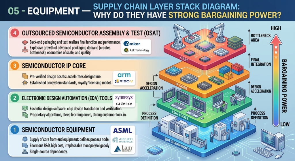
Even the best foundry can’t make a chip without equipment, and even the smartest fabless company can’t start designing without EDA software and IP cores.
Equipment
| Category | Key players | Notes |
|---|---|---|
| Lithography | ASML (Netherlands) | Effective monopoly on EUV lithography systems |
| Deposition & etch | Applied Materials, Lam Research (US) | Core tools for building up and carving away thin films |
| Coating, development, cleaning | Tokyo Electron (Japan) | Dominant in pre/post-lithography process equipment |
| Metrology & defect inspection | KLA (US) | Nanometer-scale defect detection, near-monopoly |
| Test | Advantest (Japan), Teradyne (US) | Final pass/fail testing of finished chips |
Design tools & IP
| Layer | Key players | Role |
|---|---|---|
| EDA software | Synopsys, Cadence (US) | Circuit design, simulation, and verification — a near-duopoly |
| Licensed IP cores | Arm Holdings (UK) | The design foundation behind most smartphone application-processor CPU cores |
| Open IP cores | RISC-V ecosystem | Free, open instruction-set architecture — even individuals can design a chip on it |
Packaging materials & OSAT
| Component | Role | Key players |
|---|---|---|
| OSAT (outsourced assembly & test) | Handles packaging and final testing | ASE (Taiwan), Amkor (US), JCET (China) |
| Substrate | Connects the chip to the mainboard | Ibiden, Shinko Electric (Japan), Samsung Electro-Mechanics |
| Advanced packaging | Stacks multiple chips (logic + HBM) into one package | TSMC CoWoS, Samsung I-Cube |
ASML, KLA, Synopsys, and Cadence each hold a near-monopoly in their respective niches — which is why they’re often described as having more negotiating leverage than TSMC or Samsung.
07 · Infrastructure: Why Chip Fabs Are So Thirsty and So Power-Hungry
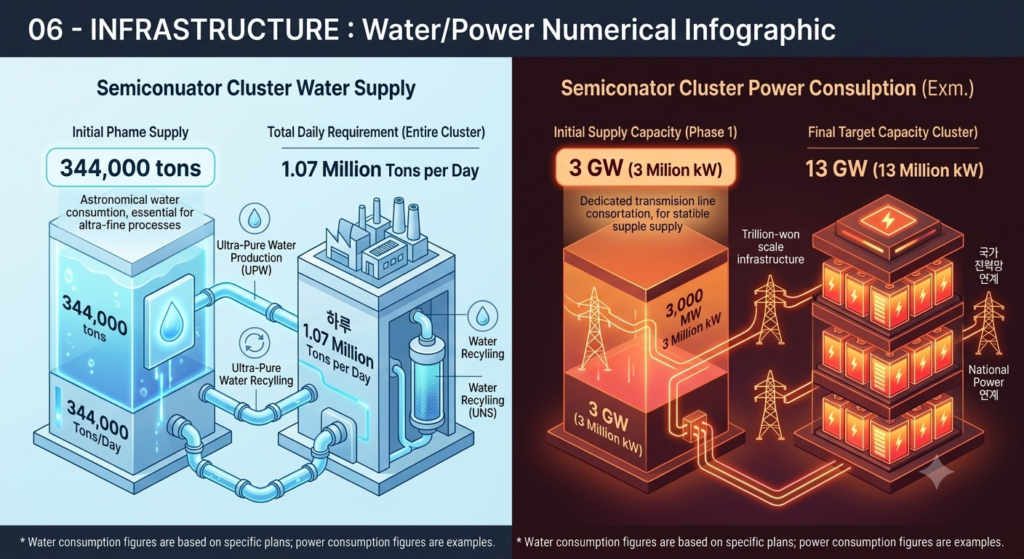
Semiconductor fabs are among the most water- and power-intensive industries on Earth, driven by two hard requirements: process precision and uninterrupted 24-hour operation.
Water — a wafer gets rinsed again and again
| Figure | Detail |
|---|---|
| Ultra-pure water yield | Producing 1 m³ of ultra-pure water can require up to 4 m³ of raw water |
| Samsung Electronics’ daily usage | Roughly 344,000 tonnes — comparable to the domestic water use of a city of a million people |
| Yongin cluster (once complete) | Expected to need roughly 1.07 million tonnes per day |
| Korea, 2030 projection | The semiconductor sector as a whole is projected to need about 3.25 million tonnes per day |
A 2021 drought in Tainan, Taiwan forced TSMC to draw on agricultural water reserves, and a 2021 cold snap in Austin, Texas halted Samsung’s ultra-pure water process, causing an estimated loss in the hundreds of millions of dollars.
Power — a one-second outage can scrap an entire wafer lot
| Factor | Explanation |
|---|---|
| EUV lithography systems | A single machine can draw as much power as a small town |
| 24-hour uninterrupted operation | A power outage destroys every wafer mid-process |
| Cleanroom HVAC | Maintaining precise temperature, humidity, and particulate control consumes enormous power |
| Process miniaturization | Below 2nm, a single wafer can pass through more than 2,000 process steps |
08 · Downstream: Where Chips Actually End Up
| Product | Main chip types | Core requirements |
|---|---|---|
| Smartphones | Application processor (CPU+GPU+NPU), image sensor, PMIC | Low power, thermal management, on-device AI |
| Laptops/PCs | CPU, GPU, DRAM, SSD (NAND) | Balance of performance and battery life |
| Data center servers | Server CPU, AI GPU/TPU, HBM | Extreme performance, parallel processing, cooling |
| EVs / autonomous vehicles | Automotive MCUs, power semiconductors (SiC), ADAS AI chips | Heat/vibration durability, safety certification |
| Appliances | MCU, PMIC, communication chips | Durability, low cost, low power |
| Robots/drones | NPU, MCU, sensor-fusion chips | Real-time processing, light weight |
09 · The Rare-Earth Wildcard: Why It Matters for Chips Right Now
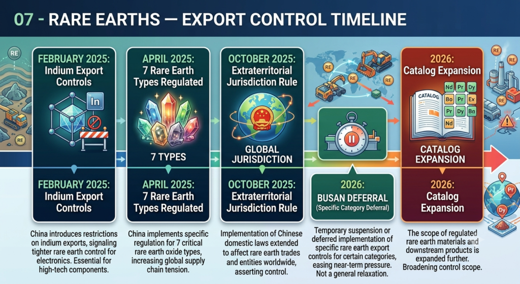
Rare earths keep making headlines in 2026, and for good reason: China controls the overwhelming majority of the world’s rare-earth processing and refining capacity, not just mining. <cite index=”7-1″>China is the leading refiner for 19 of 20 strategically important minerals, holding an average global market share of about 70%</cite>, and <cite index=”7-1″>for rare earths used in the strongest permanent magnets, China accounts for roughly 91% of global separation and refining</cite>. That processing chokepoint — not the raw ore itself — is the real leverage point.
How we got here. Beijing has escalated export controls in waves since early 2025: <cite index=”9-1″>indium licensing began in February 2025, seven heavy rare earths were added in April 2025, and a further five elements plus controls on processing technology and know-how followed in October 2025</cite>. The October 2025 measures went further than earlier rounds — <cite index=”3-1″>requiring a license for any foreign-made product containing 0.1% or more of Chinese-origin rare earths, or made using Chinese processing technology</cite>, effectively extending Chinese jurisdiction over parts of the global supply chain. After a tense standoff, <cite index=”3-1″>Beijing agreed at the end of October 2025 to suspend the new October measures for one year, in exchange for a one-year suspension of a corresponding US rule</cite> — but the earlier April 2025 controls on seven elements were left in place, so licensing requirements never fully went away.
The catalogue keeps expanding rather than shrinking. <cite index=”4-1″>China’s 2026 update to its Import-Export Licensing Catalogue added new licensing requirements for samarium, gadolinium, and lutetium compounds</cite>, materials that are foundational to electronics and clean-energy manufacturing. And this is explicitly a licensing regime, not an outright ban — <cite index=”4-1″>manufacturers can still source these materials from China, but only through licensed channels with heavier documentation and oversight</cite>.
Why chips specifically are exposed. Rare earths don’t go directly into a transistor’s silicon, but they are essential to the surrounding ecosystem: rare-earth magnets, sensors, and microelectronic components embedded inside modules and larger assemblies. Reviews aren’t applied evenly across end uses — <cite index=”8-1″>standard civilian applications tend to receive automatic approval, while advanced semiconductor manufacturing involving sub-14nm chip production faces case-by-case review, and anything tied to military AI is automatically rejected</cite>. That “surgical” gradient means consumer-electronics supply chains have mostly kept flowing, while the most advanced logic and AI chip supply chains face recurring friction and delay.
Where it’s headed. As of mid-2026 the situation remains a truce, not a resolution. <cite index=”9-1″>The suspension of the second wave of controls is set to expire in November 2026, and it isn’t yet clear whether it will be renewed</cite>. Analysts increasingly treat this not as a temporary negotiating tactic but as <cite index=”9-1″>a permanent structural feature of global trade going forward</cite>. For anyone following the semiconductor sector, the practical takeaway is this: watch the processing and refining layer, not just the mine. That’s where the real chokepoint sits, and it’s the layer that’s hardest — and slowest — for the rest of the world to replace.
10 · Breaking In: What It Actually Takes to Work in Semiconductors
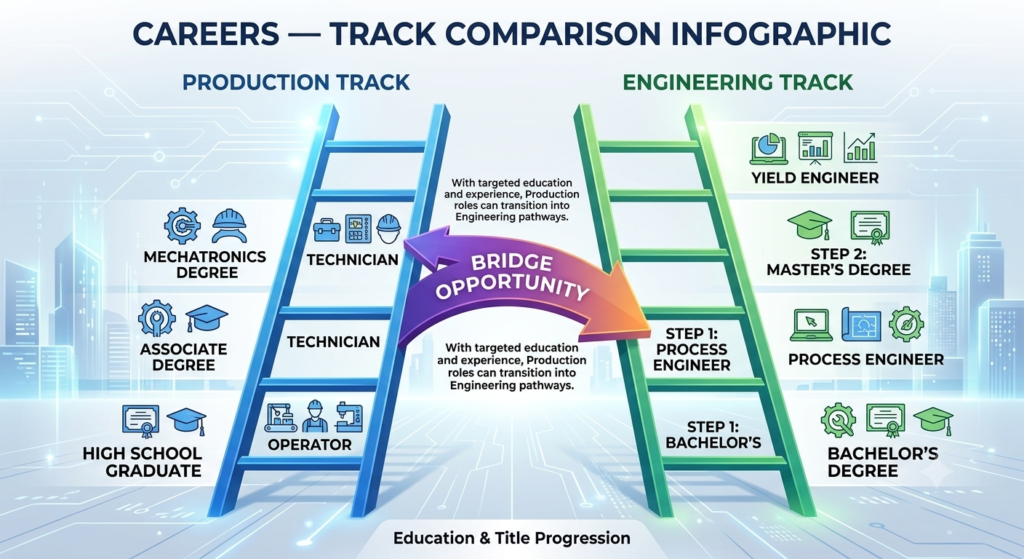
“I’m not a giant corporation and I don’t own a fab” is exactly the wrong lens. The industry has multiple entry points, and — importantly — two genuinely different career tracks that require very different preparation. People often lump them together as “semiconductor jobs,” but the production floor and the engineering bench are two different worlds.
Track 1 — Production & Manufacturing (Operators and Technicians)
This is the largest job category in the industry by headcount, and it does not require a four-year degree to get started.
- Entry point: A high school diploma (or equivalent) is often enough for entry-level operator roles — comparable in barrier-to-entry to warehouse or plant work, with paid on-the-job training.
- Next tier — technicians: Roles like process technician, equipment technician, and test technician typically call for an associate degree (2-year) in electronics technology, microelectronics, or industrial electronics, often earned at a community or technical college. On-the-job training after hiring typically runs from a few weeks to about a year.
- What the work actually involves: operating and monitoring fabrication equipment, cleanroom protocols, wafer handling, running metrology and defect-inspection tools, data logging, and troubleshooting process deviations under close safety and quality controls.
- Core skills that matter: attention to detail, comfort in a full cleanroom suit for extended periods, basic electronics/mechanical literacy, reliability, and clear written communication with engineers.
- Where it can lead: senior technician roles, and — with further study — a bridge into engineering. It’s a genuinely common path: technicians who complete a bachelor’s degree while working often move into process or materials engineering roles.
Track 2 — Engineering & Technical Roles
This track designs the process itself, rather than running it, and generally requires a four-year degree as the floor, not the ceiling.
- Minimum credential: A bachelor’s degree in electrical/computer engineering, chemical engineering, materials science, physics, or applied physics. A master’s degree is common for advanced roles (device engineering, integration engineering, R&D).
- Representative roles: process engineer (develops and tunes the fabrication steps), device/integration engineer (owns the end-to-end manufacturing flow for a chip), yield engineer (hunts down why some wafers fail), materials engineer, IC/design engineer, and equipment/field-service engineer (installs, maintains, and troubleshoots fab tools — sometimes travels between client sites).
- Core knowledge base: semiconductor physics and materials science, photolithography/etch/deposition/metrology process fundamentals, statistics and design-of-experiments (used constantly for yield analysis), and — for design-side roles — EDA tools (Synopsys/Cadence-class software) and increasingly RISC-V or other IP-core design flows.
- Pay and demand context: industry sources place manufacturing-technician pay roughly in the $40,000–$70,000 range in the US, versus roughly $70,000–$150,000+ for engineering roles, though this varies enormously by country, seniority, and specialty — treat these as rough US benchmarks, not global figures.
The Bridge Between the Two Tracks
The two tracks aren’t sealed off from each other. It’s common — and increasingly encouraged by employers facing talent shortages — for technicians to earn a bachelor’s degree part-time and move into engineering, or for new engineering hires to spend their first months learning the floor from experienced technicians. If you’re choosing where to start, the honest framing is: production roles get you into the industry faster and with less upfront cost; engineering roles take longer to enter but open a wider set of doors once you’re in.
11 · So What Can an Ordinary Person Actually Do With All This?
“I’m not a conglomerate and I don’t have a factory” is a common — and, as the section above shows, somewhat outdated — assumption. The industry has more entry points than people think, at very different levels of commitment.
1. Build your own test chip through a multi-project wafer (MPW) program (difficulty: ★★☆☆☆) Open-source and shared-fabrication programs such as Efabless, Tiny Tapeout, and SkyWater’s 130nm process let individuals fabricate an actual silicon prototype. It’s even possible to design your own core on RISC-V.
2. Build semiconductor design or verification software (difficulty: ★★★☆☆) Defect-detection AI, process-data analytics tools, and yield-prediction models are areas that are approachable purely through software skills, without ever touching a fab.
3. Create specialized content, education, or a newsletter about the industry (difficulty: ★☆☆☆☆) Because information asymmetry in this industry is large, simply explaining process technology, the materials supply chain, and investment trends in plain language is, by itself, a viable business.
4. Go from embedded prototype to small-batch contract manufacturing (difficulty: ★★☆☆☆) Building a prototype on an Arduino or FPGA board and then moving to small-batch production is the most common hardware-startup path.
5. Find a niche in the materials/parts/equipment supply chain (difficulty: ★★☆☆☆) There’s real room for smaller B2B businesses in specialty chemicals distribution, component resale, used-equipment trading, and certification/compliance services.
6. Use your understanding of the industry to inform investment research (difficulty: ★★★☆☆) There are investable opportunities across materials suppliers, foundries, fabless companies, and thematic ETFs — but be aware that this sector is prone to sharp, sentiment-driven swings. (This is background information, not investment advice.)
#GPU #NPU #TPU #AIChips #MemoryChips #DRAM #Foundry #Fabless #EUVLithography #ASML #ChipManufacturing #WaferFabrication #SemiconductorJobs #ExportControls #RareEarthExportControls #TechSupplyChain #SiliconWafer #Semiconductor #Equipment #RareEarths #ChipWar #ASML #TSMC #TechCareers